PCB Layout: Ground Planes, Return Paths, and Signal Integrity
Signal Integrity is Everything
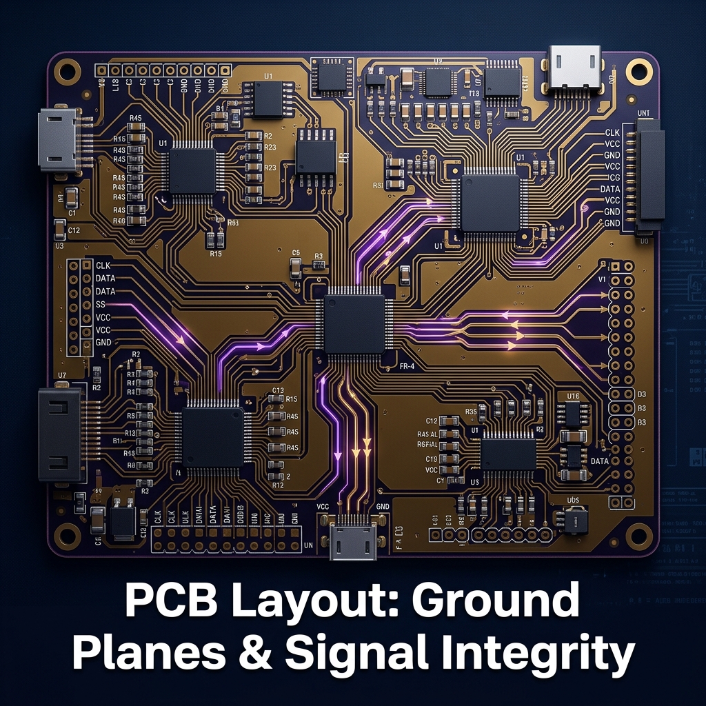
As switching speeds increase in modern electronics, a PCB trace is no longer just a simple wire; it becomes a transmission line. How you route your traces—and more importantly, how you handle your ground—determines whether your board will work perfectly or fail EMI compliance.
The Myth of "Ground"
We often think of ground as an infinite sink where current simply disappears. In reality, current must always return to its source. A signal is a closed loop.
High-Frequency Return Paths
At DC or very low frequencies, return current takes the path of least resistance (usually a straight line). However, at high frequencies, return current takes the path of least inductance, which is directly underneath the signal trace on the adjacent ground plane.
If you break the ground plane underneath a high-speed trace (e.g., routing over a split plane or a void), the return current is forced to take a longer path. This creates a large loop area, increasing inductance, radiating EMI, and severely degrading signal integrity.
Best Practices for PCB Layout
- Unbroken Ground Planes: Always provide an unbroken, continuous ground plane underneath your high-speed signals.
- Impedance Matching: Use tools like the DevtronTech Microstrip Calculator to calculate the correct trace width to hit your 50Ω target.
- Via Stitching: If a signal transitions between layers and changes its reference plane, place a "stitching via" nearby to allow the return current to jump between the planes.