DevtronTech Blog

Insights into Software, Electronics, and GeoSpatial Engineering

Temperature Monitoring Options for XC7A100T FPGA Electronics

Temperature Monitoring Options for XC7A100T FPGA

Temperature Monitoring Options for XC7A100T FPGA

When designing with the Xilinx Artix-7 XC7A100T FPGA (and similar ICs), temperature monitoring is critical for thermal management, ensuring system reliability, and preventing thermal damage. There are two primary methods for monitoring the die temperature of this FPGA:

1. Internal XADC (System Monitor)

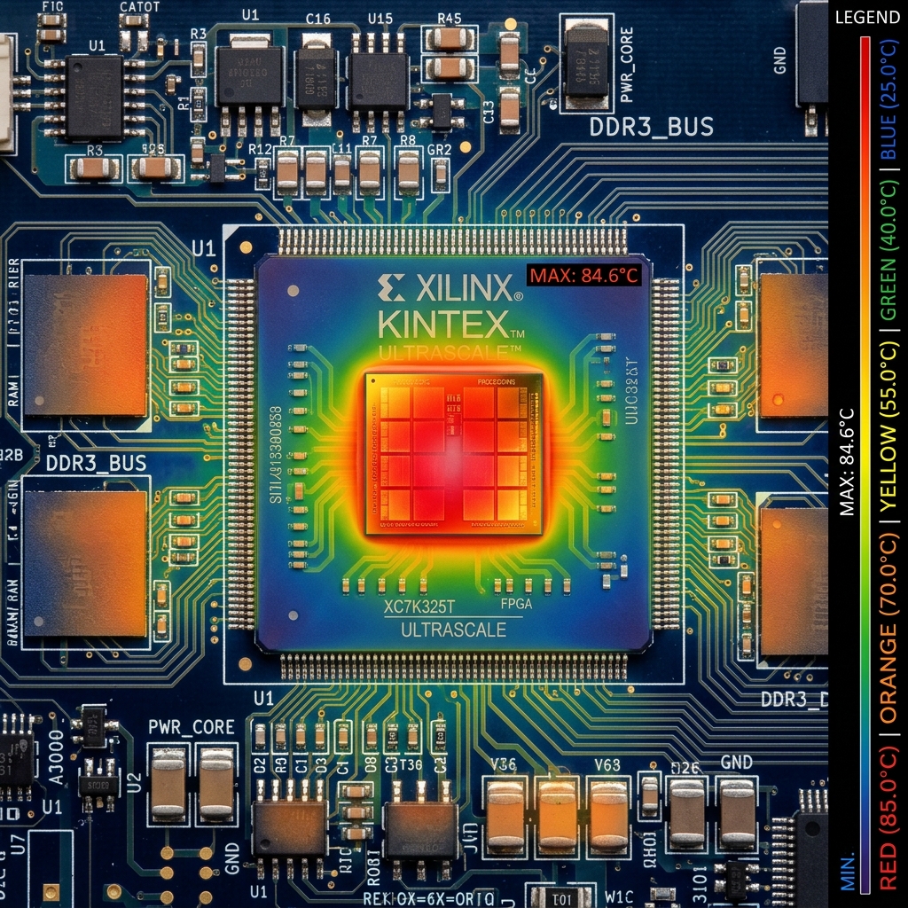
The Artix-7 family features an integrated dual 1 MSPS, 12-bit Analog-to-Digital Converter (XADC) block.

- How it works: The XADC includes a dedicated on-chip temperature sensor located directly on the silicon die. It continuously measures the core die temperature and digitizes the readings.

- Usage: This temperature data can be accessed internally by the FPGA's own logic (e.g., via the DRP - Dynamic Reconfiguration Port) or accessed externally via the JTAG interface.

- Advantages: It requires zero external components, simplifying the PCB design and reducing the Bill of Materials (BOM). It also allows the FPGA to proactively monitor its own thermal state and trigger internal logic, such as alarms or throttling, if temperatures rise too high.

2. External Thermal Diode (DXP/DXN Pins)

The FPGA also exposes a direct connection to a physical PN junction (a thermal diode) fabricated on the die via the DXP (Diode Excite Positive / Anode) and DXN (Diode Excite Negative / Cathode) pins.

- How it works: An external hardware temperature monitoring IC (such as those made by TI, Maxim, or Analog Devices) connects to these pins. The external IC injects two precise, differing currents into the diode and measures the varying forward voltage drops. The voltage difference is used to calculate a highly accurate temperature reading.

- Usage: This is typically used when the system architecture requires a central, external hardware monitor or BMC (Baseboard Management Controller) to manage the thermals of all critical components (CPU, GPU, FPGA, etc.) independently.

- Advantages: Provides true "out-of-band" temperature monitoring. The external IC can read the FPGA's temperature and spin up cooling fans or cut system power even if the FPGA's internal logic is not yet configured, is held in reset, or has locked up.

- Unused State: If external monitoring is not utilized in the design, Xilinx documentation recommends tying both the DXP and DXN pins directly to ground (GND). This prevents the unconnected pins from acting as antennas and injecting electrical noise into the substrate.

Summary

- Choose the XADC for self-contained, internal temperature monitoring without additional component cost.

- Choose the DXP/DXN thermal diode pins when relying on an external, system-level management IC for board-wide thermal control and out-of-band monitoring.

Read More
Introduction to openEMS Electronics

Introduction to openEMS

Introduction to openEMS

openEMS is a free and open-source 3D electromagnetic (EM) field solver. It utilizes the Finite-Difference Time-Domain (FDTD) method to simulate Maxwell's equations. For PCB designers and engineers working on high-speed digital or RF circuits, it serves as an accessible alternative to expensive commercial tools like Ansys HFSS, Keysight ADS, or Simbeor.

1. Core Capabilities

openEMS is highly capable of performing the rigorous analysis required for modern hardware design:

* S-Parameter Extraction: Calculates S-parameters (Insertion loss, return loss, crosstalk) for traces, vias, and connectors.

* Impedance Calculation: Determines the characteristic impedance ($Z_0$) of complex trace geometries, differential pairs, and coplanar waveguides.

* Near-Field and Far-Field Visualization: Simulates and visualizes how electromagnetic fields propagate, which is critical for identifying EMI (Electromagnetic Interference) issues and analyzing antenna radiation patterns.

* Time-Domain Reflectometry (TDR): Simulates TDR to locate impedance discontinuities along a signal path.

2. How it Works (The Workflow)

Unlike commercial EM solvers, openEMS does not have a standalone Graphical User Interface (GUI). Instead, it relies on a scripting interface.

  1. Scripting Environment: You define your simulation geometry, material properties, mesh size, and excitation ports using scripts. The primary supported languages are Python, MATLAB, and GNU Octave.
  2. AppCSXCAD (Visualization): openEMS comes with a companion viewer called AppCSXCAD. Before running the heavy simulation, you use this viewer to visually verify that your geometry, mesh, and ports have been scripted correctly.
  3. Simulation Engine: Once verified, the script calls the openEMS C++ engine to perform the FDTD simulation. This step can be computationally intensive and scales well with multi-core CPUs.
  4. Post-Processing: The output data (like voltage and current over time) is pulled back into your Python/MATLAB script, where you can apply Fast Fourier Transforms (FFT) to convert it into frequency-domain data (like S-parameters) and plot the results.

3. PCB Workflow and Integration

Simulating an entire complex PCB (like an FPGA board) in a 3D EM solver is extremely difficult and computationally expensive. The best practice is to isolate critical sections (like a single high-speed memory trace or a differential pair).

To bridge the gap between EDA tools (like Altium Designer) and openEMS, the community has developed helper tools:

* gerber2ems: An open-source tool developed by Antmicro. It automates the conversion of standard PCB manufacturing files (Gerbers) into the geometric formats required by openEMS. This prevents the engineer from having to manually script the exact coordinates of every copper trace.

* Workflow:

1. Export Gerbers from Altium for the specific layers/traces you want to analyze.

2. Use gerber2ems to translate the geometry.

3. Use a Python script to define the mesh, attach ports to the ends of the traces, and run the openEMS simulation.

4. Pros and Cons

Pros:

* Cost: 100% Free and open-source.

* Transparency: Full control over the simulation parameters and mesh.

* Automation: Because it is script-driven, it is highly suitable for automated parameter sweeps and optimization loops.

Cons:

* Steep Learning Curve: Requires programming knowledge (Python/MATLAB) and a strong understanding of EM simulation principles (like how to define a proper FDTD mesh and absorbing boundary conditions).

* No Native PCB Importer: Lacks the seamless "import board and click simulate" experience of commercial SI/PI tools.


*For more information, documentation, and tutorials, visit the official openEMS project page: [https://openems.de](https://openems.de)*

Read More
Introduction to Hybrid Output Capacitors Electronics

Introduction to Hybrid Output Capacitors

Introduction to Hybrid Output Capacitors

In modern hardware engineering, particularly when designing Power Delivery Networks (PDNs) for high-performance ICs like FPGAs, the term "Hybrid Capacitor" generally refers to Conductive Polymer Hybrid Aluminum Electrolytic Capacitors.

These advanced components bridge the gap between two older technologies, offering a "best of both worlds" solution for switching regulator output stages.


1. What is a Hybrid Polymer Capacitor?

A physical hybrid capacitor combines two different materials within the same capacitor casing:

  1. Solid Conductive Polymer: Provides extremely low Equivalent Series Resistance (ESR) and excellent high-frequency performance.
  2. Liquid Electrolyte: Provides high capacitance density, lower leakage current, and a unique "self-healing" property where the liquid can repair micro-damage to the dielectric layer over time.

Key Advantages for Power Supply Design

* Massive Ripple Current Handling: Thanks to the ultra-low ESR of the solid polymer, these capacitors can absorb massive amounts of switching ripple current without overheating.

* No DC Bias Effect: Unlike Ceramic Capacitors (MLCCs)—which can lose up to 70% of their stated capacitance when a DC voltage is applied—hybrid capacitors maintain their full capacitance under load.

* No Piezoelectric Noise: Ceramic capacitors can physically vibrate and emit an audible whine under high ripple. Hybrid capacitors do not suffer from this.

* Space Efficiency: Because one hybrid capacitor has such high performance, a single unit can often replace a bulky array of 4 to 5 standard wet electrolytic capacitors, saving massive amounts of PCB area.


2. Component vs. Network (An Important Distinction)

It is crucial to differentiate between a physical hybrid component and a circuit topology concept:

* Hybrid Polymer Capacitor (Component): A single physical part you solder to the board that contains mixed liquid/solid materials inside.

* Hybrid Capacitor Network (Circuit Topology): A design strategy where you place *different types* of physical capacitors in parallel on your schematic.

* *Example:* Placing a large bulk Aluminum Electrolytic capacitor (high capacitance, high ESR) in parallel with tiny Ceramic MLCCs (low capacitance, ultra-low ESR).


3. Stability: The Load Pole and ESR Zero

When designing a buck converter, the output capacitors interact with the load to affect the stability of the control loop.

* The Load Pole: In control theory, a "pole" is a frequency where the power supply's ability to react starts to roll off (lag). The combination of the output capacitance ($C_{out}$) and the resistance of the FPGA load ($R_{load}$) acts as an RC low-pass filter, creating this pole.

* The ESR Zero: The Equivalent Series Resistance (ESR) of the capacitor creates a "Zero" (the mathematical opposite of a pole), which actually helps push back against the phase delay and improves stability.

When you use a Hybrid Capacitor Network (mixing different types of capacitors in parallel), calculating the exact frequencies of the Load Pole and ESR Zero becomes highly complex. IC manufacturers (like Texas Instruments) provide complex application notes specifically to help engineers calculate these values so they can correctly tune the buck converter's compensation network and prevent the power supply from oscillating.


4. Industry Standard Part Numbers

If you are looking to specify physical Hybrid Polymer Capacitors for a 5V, 12V, or 24V rail on an FPGA board, here are the industry-standard go-to components (assuming a common 25V, 100µF requirement):

* Panasonic EEH-ZA Series (e.g., EEH-ZA1E101XP): The gold standard for 105°C endurance and low ESR (30 mΩ).

* Nichicon GYA Series (e.g., GYA1E101MCQ1GS): Designed for extended operation at higher temperatures (up to 125°C).

* Rubycon PZA Series: A highly reliable alternative equivalent to the Panasonic and Nichicon offerings.

Read More
Building an Auto-Shutdown System with the MCP2221, Python, and a Delay Circuit Electronics

Building an Auto-Shutdown System with the MCP2221, Python, and a Delay Circuit


title: "Building an Auto-Shutdown System with the MCP2221, Python, and a Delay Circuit"

category: "Electronics"

date: "2026-06-17"

description: "Learn how to use the MCP2221 USB-to-I2C/UART/GPIO breakout board alongside a custom delay circuit and Python to safely auto-shutdown a Windows system."


Building an Auto-Shutdown System with the MCP2221, Python, and a Delay Circuit

In many embedded applications, arcade cabinets, or remote kiosks, safely powering down a Windows PC without a keyboard or mouse is a common challenge. Hard-cutting the power can corrupt the operating system, but relying on users to manually navigate to the start menu isn't always practical.

To solve this, we recently designed and implemented a hardware-software bridge using the Microchip MCP2221 board, a custom delay circuit, and a lightweight Python script. Here’s a look at how we built this auto-shutdown system and how you can replicate it for your own projects.


The Hardware: MCP2221 and the Delay Circuit

The [MCP2221](https://www.microchip.com/en-us/product/MCP2221A) is a fantastic, low-cost USB-to-UART/I2C serial converter that also includes general-purpose input/output (GPIO) pins. Because it connects directly via USB, it acts as the perfect bridge between physical hardware switches and our PC's software.

The Problem with Immediate Shutdowns

If a user flips a physical "Power Off" toggle switch, we don't want the PC's power supply to immediately cut out. Windows needs time to close background processes, save states, and gracefully halt.

The Solution: An MCU-Controlled Delay

To handle this, we implemented a custom auto-shutdown system where a Microcontroller Unit (MCU) bridges the physical switch and the PC.

When the physical power switch is thrown:

  1. The MCU detects the change and begins a hardware countdown before it actually cuts the mains power to the PC.
  2. Adjustable Delays: The user can easily adjust the required delay time (e.g., 10, 30, or 60 seconds) in the MCU to perfectly match how long their specific Windows machine takes to halt.
  3. Simultaneously, the MCU signals the PC by driving one of the MCP2221's GPIO pins LOW. We are reading the status directly from the MCU pin to the MCP2221 GPIO.

This gives our software a 30-second window to detect the switch throw and command Windows to shut down gracefully before the physical power is severed.

Note: If you connect the GPIO pin directly to a High (or Low) signal driven by the MCU, you do not need to add an external pull-up resistor to the circuit. This keeps the hardware footprint incredibly minimal!

The Software: Python and GPIO Polling

To detect the GPIO state change, we wrote a background Python service. The script relies on the EasyMCP2221 library (or Adafruit's Blinka) to poll the USB device, and the built-in os module to trigger the Windows shutdown.

1. Setting up the Environment

First, install the required library:

pip install EasyMCP2221

2. The Python Script

Here is the core logic that runs in the background on the Windows machine. It continuously polls GP3 on the MCP2221. When it detects that the delay circuit has pulled the pin low, it fires the Windows shutdown command.

import time
import os
import EasyMCP2221

# Connect to the MCP2221 device
try:
    mcp = EasyMCP2221.Device()
    print("MCP2221 Connected Successfully.")
except Exception as e:
    print(f"Failed to connect to MCP2221: {e}")
    exit(1)

# Configure GP3 as a GPIO Input
mcp.set_pin_function(gp3="GPIO_IN")

print("Monitoring power switch on GP3...")

while True:
    try:
        # Read the status of all GPIO pins
        status = mcp.GPIO_read()
        
        # Check if the delay circuit has pulled GP3 Low (0)
        # Assuming an Active-Low configuration
        if status['gp3'] == 0:
            print("Power switch toggled! Initiating graceful shutdown...")
            
            # Send the Windows shutdown command
            # /s = shutdown, /t 0 = zero second delay in Windows 
            # (since our hardware circuit gives us the time we need)
            os.system("shutdown /s /t 0")
            
            # Break the loop so we don't spam the command
            break
            
        # Poll every 500ms to avoid high CPU usage
        time.sleep(0.5)
        
    except Exception as e:
        print(f"Error reading MCP2221: {e}")
        time.sleep(1)

How It All Comes Together

When the system is running, the workflow looks like this:

  1. User turns off the main switch.
  2. The MCU detects this and begins its user-configured physical hardware countdown.
  3. The MCU simultaneously pulls the MCP2221 GP3 pin LOW.
  4. Within 500ms, our Python script detects the LOW state.
  5. Python executes shutdown /s /t 0.
  6. Windows gracefully logs out, saves files, and powers down the OS.
  7. Finally, the MCU's adjustable delay timer expires and it completely cuts the AC mains power, ensuring zero phantom draw.

Conclusion

By combining a simple MCU-controlled delay with the MCP2221, we were able to create an incredibly robust and customizable auto-shutdown system. The user can adjust the delays as required, the MCP2221 handles the USB communication natively, and Python makes the Windows integration a breeze.

Read More
Modern C++ (C++17/20) Best Practices for Embedded Systems Software

Modern C++ (C++17/20) Best Practices for Embedded Systems

Bringing Embedded Systems into the 21st Century

Embedded systems have traditionally been written in pure C. However, modern C++ (specifically C++17 and C++20) offers incredible features that improve type safety, readability, and abstraction without sacrificing runtime performance. In fact, many modern C++ features resolve entirely at compile time (Zero-Cost Abstractions).

1. constexpr for Compile-Time Evaluation

Why calculate a lookup table at runtime when the compiler can do it for you? constexpr guarantees that expressions are evaluated at compile time, saving precious MCU cycles.

constexpr float pi = 3.1415926f;

// Evaluated entirely at compile time
constexpr int degrees_to_adc(float deg) {
    return static_cast((deg / 360.0f) * 4096);
}

2. std::array and std::span

Stop using raw C-arrays that decay to pointers and lose their size information. std::array provides the same performance as a raw array but with boundary checks and STL iterator support.

std::span (C++20) provides a safe, non-owning view over a contiguous block of memory, perfect for passing buffers to DMA functions without pointer-arithmetic bugs.

3. Auto and Structured Bindings (C++17)

Make your code cleaner when returning multiple values from sensor reading functions.

struct SensorData { float temp; float humidity; };

SensorData read_bme280() { return {24.5f, 50.2f}; }

// C++17 Structured Binding
auto [temperature, humidity] = read_bme280();

4. Don't Fear Templates, but Fear RTTI and Exceptions

Templates are resolved at compile time and cost nothing at runtime (though they can increase code size). However, you should generally disable Exceptions (-fno-exceptions) and Run-Time Type Information (-fno-rtti) in embedded environments, as they introduce unpredictable overhead and bloat the binary.

Read More
Getting Started with Dear ImGui for C++ Desktop Apps Software

Getting Started with Dear ImGui for C++ Desktop Apps

Immediate Mode GUIs for Tools

If you are building game engines, internal developer tools, or hardware debuggers in C++, traditional retained-mode GUI frameworks (like Qt or wxWidgets) can feel incredibly heavy and complex to integrate. Enter Dear ImGui.

What is Immediate Mode GUI?

In a retained-mode GUI, you create an object (like a Button), add it to a hierarchy, and rely on an event loop to call your callbacks. State is stored in the UI tree.

In an immediate-mode GUI, there is no UI state stored. You simply call the UI drawing commands every single frame inside your main game loop. If you want a button, you call an if (ImGui::Button("Click Me")) statement.

Why Dear ImGui?

  • Zero integration friction: It is renderer-agnostic. It just outputs vertex buffers. You can hook it up to OpenGL, DirectX, Vulkan, or Metal easily.
  • State management is trivial: Since the UI is redrawn every frame based on your app's variables, you never have data synchronization bugs.
  • Fast to write: Creating complex debug panels takes minutes, not hours.

A Quick Example

// Inside your main loop, every frame:
ImGui_ImplOpenGL3_NewFrame();
ImGui_ImplGlfw_NewFrame();
ImGui::NewFrame();

// Build the UI
ImGui::Begin("Debug Panel"); 
static float f = 0.0f;
ImGui::SliderFloat("Speed", &f, 0.0f, 1.0f);
if (ImGui::Button("Reset")) {
    f = 0.0f;
}
ImGui::End();

// Render
ImGui::Render();
ImGui_ImplOpenGL3_RenderDrawData(ImGui::GetDrawData());
Read More
Building a High-Performance Node.js C++ Addon with node-addon-api Software

Building a High-Performance Node.js C++ Addon with node-addon-api

Breaking the V8 Speed Limit

Node.js is fantastic for I/O bound tasks, but its single-threaded JavaScript execution can struggle with heavy CPU-bound workloads like image processing, encryption, or complex mathematical simulations. The solution? Write the heavy lifting in C++ and expose it to Node.js as a native addon.

What is N-API?

Historically, C++ addons were tied directly to the V8 engine's API, meaning they broke every time Node.js updated V8. N-API (Node-API) provides an ABI-stable layer, ensuring your compiled binary works across Node.js versions without recompilation.

node-addon-api is the modern, header-only C++ wrapper around N-API that makes writing addons significantly easier by utilizing C++ object models.

Creating Your First Addon

1. Initialize and install dependencies:

npm init -y
npm install node-addon-api
npm install -g node-gyp

2. Create a binding.gyp file to configure the build.

3. Write the C++ code (main.cpp):

#include <napi.h>

// The C++ function
Napi::String HelloMethod(const Napi::CallbackInfo& info) {
    Napi::Env env = info.Env();
    return Napi::String::New(env, "Hello from C++!");
}

// Module initialization
Napi::Object Init(Napi::Env env, Napi::Object exports) {
    exports.Set(Napi::String::New(env, "hello"),
                Napi::Function::New(env, HelloMethod));
    return exports;
}

NODE_API_MODULE(hello_addon, Init)

4. Build it using node-gyp configure build and require it in Node.js!

Read More
Visualizing GeoJSON Data on the Web using JavaScript GeoSpatial

Visualizing GeoJSON Data on the Web using JavaScript

Bringing Data to Life

Once you have your geographic data in GeoJSON format, rendering it beautifully in the browser is straightforward thanks to modern mapping libraries.

Choosing a Library

  • Leaflet.js: Lightweight, easy to learn, perfect for simple maps and smaller GeoJSON datasets (under 10,000 features). Uses DOM elements (SVG/Canvas) to render.
  • MapLibre GL JS / Mapbox GL JS: WebGL-accelerated. Incredibly fast, capable of rendering millions of points smoothly. Requires data to be styled using layers and sources rather than iterating over arrays.

A Simple MapLibre Implementation

Here is how you add a GeoJSON source and a polygon layer using MapLibre:

const map = new maplibregl.Map({
    container: 'map', // HTML div id
    style: 'https://demotiles.maplibre.org/style.json',
    center: [-74.006, 40.712], // Longitude, Latitude
    zoom: 10
});

map.on('load', () => {
    // 1. Add the GeoJSON as a data source
    map.addSource('my-data', {
        'type': 'geojson',
        'data': 'https://example.com/data.json'
    });

    // 2. Add a visual layer connected to the source
    map.addLayer({
        'id': 'polygons-fill',
        'type': 'fill',
        'source': 'my-data',
        'paint': {
            'fill-color': '#088',
            'fill-opacity': 0.6
        }
    });
});

For large datasets, always consider converting your GeoJSON into Vector Tiles (e.g., using Tippecanoe) before serving them to the client!

Read More
How to Process and Convert Large Shapefiles Efficiently in Node.js GeoSpatial

How to Process and Convert Large Shapefiles Efficiently in Node.js

Handling Big Data in Node.js

Converting a small Shapefile to GeoJSON is easy. But what happens when a user uploads a 500MB zipped Shapefile with millions of polygons? Loading it all into memory with JSON.parse() will cause V8 to throw a FATAL ERROR: Ineffective mark-compacts near heap limit Allocation failed - JavaScript heap out of memory.

The Solution: Streaming

To process massive geospatial datasets in Node.js, you must use streams. Instead of loading the entire file, you read it chunk by chunk.

Step-by-step Approach

  1. Unzip using streams: Use libraries like unzipper or yauzl to extract the .shp and .dbf files without loading the zip into memory.
  2. Stream the Shapefile: Use the shapefile npm package. Its open() method returns a reader that you can iterate over asynchronously.
  3. Write to disk incrementally: Don't build a massive JavaScript array. Instead, open a fs.createWriteStream and write the GeoJSON structure manually, streaming each feature into the file.
import shapefile from 'shapefile';
import fs from 'fs';

async function streamToGeoJSON(shpPath) {
    const outStream = fs.createWriteStream('out.json');
    outStream.write('{"type":"FeatureCollection","features":[');
    
    let first = true;
    const source = await shapefile.open(shpPath);
    
    while(true) {
        const result = await source.read();
        if (result.done) break;
        
        if (!first) outStream.write(',');
        outStream.write(JSON.stringify(result.value));
        first = false;
    }
    
    outStream.write(']}');
    outStream.end();
}

This approach uses almost zero RAM, allowing Node.js to process Gigabyte-sized maps efficiently.

Read More
Demystifying Coordinate Reference Systems: EPSG:4326 vs EPSG:3857 GeoSpatial

Demystifying Coordinate Reference Systems: EPSG:4326 vs EPSG:3857

Why is my map rendering in the ocean?

If you've ever plotted data on a map and found your points ending up off the coast of Africa (Null Island), you have encountered a Coordinate Reference System (CRS) mismatch. The two most important EPSG codes for web developers are EPSG:4326 and EPSG:3857.

EPSG:4326 (WGS 84)

This is the geographic coordinate system used by GPS. It represents locations using Latitude and Longitude degrees on a 3D model of the Earth (a datum).

  • Units: Degrees.
  • Example: London is [51.5074° N, 0.1278° W].
  • Use Case: Storing data in databases, GeoJSON, and capturing GPS coordinates.

EPSG:3857 (Web Mercator)

This is a projected coordinate system used by almost all web mapping libraries (Google Maps, OpenStreetMap, Mapbox). It takes the 3D globe and flattens it onto a 2D square. Because it's a square, it severely distorts the poles (which is why Greenland looks as big as Africa on Google Maps).

  • Units: Meters.
  • Example: London is roughly [6711514m North, 14224m West].
  • Use Case: Rendering map tiles on a flat screen.

The Golden Rule of Web Mapping

Store your data in EPSG:4326. Render your maps in EPSG:3857.

Most mapping libraries (like Leaflet or Mapbox GL JS) will automatically project your EPSG:4326 GeoJSON data into EPSG:3857 for rendering on the screen. However, if you are generating raw vector tiles on a backend server, you must mathematically project the geometries yourself using tools like proj4js or GDAL.

Read More
Shapefile vs. GeoJSON: A Developer's Guide to GIS Formats GeoSpatial

Shapefile vs. GeoJSON: A Developer's Guide to GIS Formats

The Tale of Two Formats

In the world of GIS (Geographic Information Systems) and web mapping, developers constantly encounter two dominant formats: the legacy Shapefile and the modern GeoJSON. Here is how they compare.

The ESRI Shapefile

Created by ESRI in the 1990s, the "Shapefile" is not actually a single file. It is a mandatory collection of at least three files:

  • .shp: Contains the geometry data (points, lines, polygons).
  • .shx: The index file.
  • .dbf: A dBase database file containing the attribute data (properties).
  • .prj: (Optional but critical) Defines the coordinate system.

Pros: Supported by literally every desktop GIS software. Extremely fast to read sequentially.
Cons: Cannot hold multiple geometry types in one file. File size limits (2GB). Annoying to transfer over the web because it requires zipping multiple files.

GeoJSON

GeoJSON is an open standard format designed for representing simple geographical features using JSON (JavaScript Object Notation).

Pros: Human-readable. A single text file. Natively supported by web browsers, JavaScript mapping libraries (Leaflet, Mapbox), and NoSQL databases like MongoDB and Postgres/PostGIS.
Cons: File sizes can become massive compared to binary formats, making them slow to parse if not simplified or served via vector tiles.

The Verdict

Use Shapefiles when storing raw data, archiving, or working in desktop tools like QGIS or ArcGIS. Convert to GeoJSON when you need to transmit data via a REST API or render it on a web map.

Read More
Linux Networking Cheat Sheet: Commands Every Developer Should Know Software

Linux Networking Cheat Sheet: Commands Every Developer Should Know

The DevOps & Backend Networking Toolkit

When things break in production, knowing how to debug the network is a superpower. Here are the essential Linux networking commands.

Checking Interfaces and IP Addresses

Forget ifconfig, the modern way is the ip command.

ip addr show       # List all interfaces and IPs
ip link show       # Show link status (up/down)
ip route show      # View the routing table

Finding Open Ports and Listening Services

Use ss (socket statistics) instead of netstat.

ss -tulpn          # Show listening TCP/UDP ports and the process using them
                   # (Requires root/sudo to see process names)

Testing Connectivity and DNS

ping 8.8.8.8       # Test ICMP connectivity
traceroute google.com # Show the path packets take to a host
dig example.com    # Perform a DNS lookup
nc -vz host 80     # Use Netcat to check if a specific port is open

Packet Sniffing

When you need to see exactly what is going over the wire.

tcpdump -i eth0    # Capture all traffic on eth0
tcpdump port 80    # Capture HTTP traffic only
tcpdump src 1.2.3.4 # Capture traffic from a specific IP

Firewall Rules (iptables / ufw)

sudo iptables -L -v -n  # List all current firewall rules
sudo ufw status verbose # If using Uncomplicated Firewall (Ubuntu)
Read More
Advanced C Programming Cheat Sheet Software

Advanced C Programming Cheat Sheet

Mastering C for Systems Programming

While C is a small language, mastering its nuances is essential for writing robust system-level code, OS kernels, and embedded firmware.

1. Pointers to Functions

Function pointers allow you to pass functions as arguments, enabling callbacks and state machines.

// Define a function pointer type
typedef int (*math_func)(int, int);

int add(int a, int b) { return a + b; }
int mul(int a, int b) { return a * b; }

int main() {
    math_func op = add;
    printf("Result: %d\n", op(5, 3)); // Prints 8
}

2. Struct Packing and Alignment

By default, compilers pad structs to align members to memory boundaries for performance. In embedded systems or networking, you often need to disable this.

// Use #pragma pack or __attribute__((packed))
struct __attribute__((packed)) NetworkHeader {
    uint8_t version;
    uint16_t length;
};

3. Bit Manipulation

Setting, clearing, and toggling bits is the bread and butter of embedded C.

#define BIT(x) (1 << (x))
uint32_t reg = 0;
reg |= BIT(3);  // Set bit 3
reg &= ~BIT(3); // Clear bit 3
reg ^= BIT(3);  // Toggle bit 3

4. The 'volatile' Keyword

Tells the compiler that a variable's value can change at any time without any action being taken by the code nearby (e.g., hardware registers or variables modified inside an ISR). It prevents the compiler from optimizing away reads/writes.

Read More
Protocol Deep Dive: I2C vs. SPI vs. UART for Embedded Engineers Electronics

Protocol Deep Dive: I2C vs. SPI vs. UART for Embedded Engineers

Choosing the Right Serial Protocol

Embedded systems rely heavily on serial communication to talk to sensors, memory, and other microcontrollers. The big three are UART, I2C, and SPI. Knowing when to use which is crucial.

1. UART (Universal Asynchronous Receiver-Transmitter)

Wires: 2 (TX, RX) + Ground
Speed: Low to Medium (typically up to 1-3 Mbps)

UART is asynchronous, meaning there is no shared clock signal. Both devices must agree on a baud rate beforehand. It is point-to-point (one to one). It's incredibly simple and robust, making it the standard for debug consoles and long-distance serial links (like RS-232/RS-485).

2. I2C (Inter-Integrated Circuit)

Wires: 2 (SDA, SCL) + Ground
Speed: Low to Medium (100 kHz, 400 kHz, up to 3.4 Mbps in high-speed mode)

I2C uses a multi-master, multi-slave architecture. A master generates the clock (SCL) and addresses specific slaves using a 7-bit address. Because it requires pull-up resistors and relies on open-drain pins, its speed is limited by capacitance. It is perfect for connecting multiple low-speed sensors on the same board without using up all your MCU pins.

3. SPI (Serial Peripheral Interface)

Wires: 4 (MOSI, MISO, SCK, CS) + Ground
Speed: High (often 10s of Mbps)

SPI is synchronous and uses dedicated lines for sending and receiving data simultaneously (full-duplex). There is no addressing overhead; the master selects a slave by pulling its specific Chip Select (CS) line low. It is fast and efficient, making it the go-to protocol for SD cards, displays, and high-speed ADCs.

Read More
PCB Layout: Ground Planes, Return Paths, and Signal Integrity Electronics

PCB Layout: Ground Planes, Return Paths, and Signal Integrity

Signal Integrity is Everything

As switching speeds increase in modern electronics, a PCB trace is no longer just a simple wire; it becomes a transmission line. How you route your traces—and more importantly, how you handle your ground—determines whether your board will work perfectly or fail EMI compliance.

The Myth of "Ground"

We often think of ground as an infinite sink where current simply disappears. In reality, current must always return to its source. A signal is a closed loop.

High-Frequency Return Paths

At DC or very low frequencies, return current takes the path of least resistance (usually a straight line). However, at high frequencies, return current takes the path of least inductance, which is directly underneath the signal trace on the adjacent ground plane.

If you break the ground plane underneath a high-speed trace (e.g., routing over a split plane or a void), the return current is forced to take a longer path. This creates a large loop area, increasing inductance, radiating EMI, and severely degrading signal integrity.

Best Practices for PCB Layout

  • Unbroken Ground Planes: Always provide an unbroken, continuous ground plane underneath your high-speed signals.
  • Impedance Matching: Use tools like the DevtronTech Microstrip Calculator to calculate the correct trace width to hit your 50Ω target.
  • Via Stitching: If a signal transitions between layers and changes its reference plane, place a "stitching via" nearby to allow the return current to jump between the planes.
Read More
Power Delivery Networks (PDN): Designing Stable Supplies for High-Speed ICs Electronics

Power Delivery Networks (PDN): Designing Stable Supplies for High-Speed ICs

The Importance of a Good PDN

In high-speed digital designs (like microprocessors, FPGAs, and fast memory), power consumption isn't static. It happens in rapid bursts. If the power supply cannot deliver current quickly enough, the voltage drops (voltage droop), which can cause the IC to crash or corrupt data.

A Power Delivery Network (PDN) is the entire system from the voltage regulator (VRM) to the IC die, including the PCB traces, vias, and decoupling capacitors.

The Goal: Target Impedance

The primary goal of PDN design is to maintain the impedance of the power network below a specific Target Impedance across a wide range of frequencies (from DC up to hundreds of MHz or GHz).

Key Components of a PDN

  • Voltage Regulator Module (VRM): Good for low frequencies (DC up to a few hundred kHz).
  • Bulk Capacitors (e.g., Tantalum, Electrolytic): Provide energy for frequencies up to a few MHz.
  • Decoupling Capacitors (MLCCs): Small ceramic capacitors placed as close as possible to the IC power pins. These supply instantaneous current for high-frequency transients.
  • PCB Planes: Power and Ground planes placed on adjacent layers create a large, distributed capacitance with very low inductance, handling the highest frequency requirements.

Best Practices for Layout

Place decoupling caps as close to the power pins as possible to minimize trace inductance. Use multiple vias to connect capacitor pads to internal power and ground planes to reduce mounting inductance.

Read More
Op-Amps and Their Use Cases: A Guide for Beginners Electronics

Op-Amps and Their Use Cases: A Guide for Beginners

Introduction to Operational Amplifiers

Operational Amplifiers (Op-Amps) are the workhorses of analog electronics. They are highly versatile integrated circuits that can perform mathematical operations, amplify signals, filter noise, and serve as buffers.

Common Op-Amp ICs

  • LM358: A very common, cheap dual op-amp. It's not a rail-to-rail op-amp but is excellent for basic, low-frequency tasks and DC applications.
  • NE5532: Known for low noise, making it the industry standard for high-fidelity audio equipment.
  • TL072: Features JFET inputs, giving it extremely high input impedance and low bias current, ideal for sensor interfacing and guitar pedals.

Key Configurations

1. Inverting Amplifier

The signal is applied to the inverting (-) input. The output is 180 degrees out of phase with the input. Gain is set by the ratio of the feedback resistor (Rf) to the input resistor (Rin): Gain = -Rf / Rin.

2. Non-Inverting Amplifier

The signal is applied to the non-inverting (+) input, while the feedback resistor network connects to the inverting input. The output is in phase with the input. Gain = 1 + (Rf / R1).

3. Voltage Follower (Buffer)

A special case of the non-inverting amplifier where the output is tied directly to the inverting input (Gain = 1). It has very high input impedance and low output impedance, used to isolate stages from loading effects.

Use the DevtronTech Op-Amp Gain Calculator to quickly find your required resistor values!

Read More
Advanced SQL Cheat Sheet Software

Advanced SQL Cheat Sheet

1. Common Table Expressions (CTEs)

CTEs allow you to create temporary result sets that can be referenced within a SELECT, INSERT, UPDATE, or DELETE statement.

WITH RegionalSales AS (
    SELECT Region, SUM(Sales) AS TotalSales
    FROM Orders
    GROUP BY Region
)
SELECT * FROM RegionalSales WHERE TotalSales > 100000;

2. Window Functions

Perform calculations across a set of table rows that are somehow related to the current row.

SELECT EmployeeName, Department, Salary,
       RANK() OVER(PARTITION BY Department ORDER BY Salary DESC) as DeptRank
FROM Employees;

3. Advanced Joins (Self Join & Cross Join)

-- Self Join Example (Finding employees and their managers)
SELECT e1.Name AS Employee, e2.Name AS Manager
FROM Employees e1
LEFT JOIN Employees e2 ON e1.ManagerID = e2.ID;

-- Cross Join Example (All possible combinations)
SELECT Colors.ColorName, Sizes.SizeName
FROM Colors CROSS JOIN Sizes;

4. JSON Data Extraction

Modern SQL databases support extracting values from JSON columns.

SELECT id, data->>'$.customer.name' AS CustomerName
FROM Orders
WHERE JSON_EXTRACT(data, '$.status') = 'shipped';

5. Indexing Best Practices

  • Composite Indexes: Order columns by cardinality (most unique first).
  • Covering Indexes: Include all columns retrieved by the query to avoid table lookups.
  • Avoid SELECT *: Only fetch columns you need to utilize indexes effectively.
Read More
Understanding Low-Side MOSFET Switching Electronics

Understanding Low-Side MOSFET Switching

What is a Low-Side Switch?

A low-side switch is placed between the load and Ground (0V). In this configuration, the load is permanently connected to the positive supply (Vcc), and the switch completes the circuit by providing a path to ground. This is the most common and simplest method of switching in hobbyist electronics and many embedded systems.

Using an N-Channel MOSFET

For low-side switching, an N-Channel MOSFET is the standard choice. Its Source is tied to Ground, and its Drain connects to the load. To turn the MOSFET ON, the Gate voltage is pulled higher than the Source (Vgs > 0). To turn it OFF, the Gate is pulled down to Ground (Vgs = 0).

Because the Source is firmly tied to ground, driving an N-Channel MOSFET from a microcontroller is very straightforward. As long as you choose a "Logic-Level" MOSFET (one that fully turns on at 3.3V or 5V Vgs), you can connect the Gate directly to an MCU pin (usually with a small series resistor to limit switching current and a pull-down resistor to prevent floating).

Pros and Cons

  • Pro: Extremely easy to drive directly from low-voltage logic circuits (microcontrollers).
  • Pro: N-Channel MOSFETs are generally cheaper, smaller, and have lower RDS(on) than P-Channel equivalents.
  • Con: The load is always "hot" (connected to Vcc). If the load wiring shorts to a grounded chassis, it will turn permanently ON, which can be dangerous.
  • Con: You lose a common ground reference for the load, which can interfere with communication protocols if the load is a smart device.
Read More
Understanding High-Side MOSFET Switching Electronics

Understanding High-Side MOSFET Switching

What is a High-Side Switch?

A high-side switch is placed between the positive power supply (Vcc) and the load. When the switch is open, the load is completely disconnected from the power source and is safely sitting at ground potential (0V). This is often preferred for safety and isolation reasons, particularly in automotive and industrial applications where loads sharing a common chassis ground must be completely de-energized when turned off.

Using a P-Channel MOSFET

For high-side switching, a P-Channel MOSFET is typically the easiest component to use. Its Source is tied to Vcc, and the Drain is connected to the load. To turn the MOSFET ON, the Gate voltage must be pulled lower than the Source voltage (Vgs < 0). To turn it OFF, the Gate is pulled up to Vcc (Vgs = 0).

Because microcontrollers operate at lower voltages (like 3.3V or 5V) compared to many loads (12V or 24V), directly driving a P-Channel MOSFET gate from a microcontroller pin can be impossible or dangerous. Therefore, a small N-channel MOSFET or NPN transistor is usually employed as a "level shifter" or gate driver to pull the P-channel gate down to ground.

Pros and Cons

  • Pro: Safer during faults. A short-to-ground fault on the load wiring will just blow a fuse, rather than turning the load permanently on.
  • Pro: Load sits at 0V when off, reducing corrosion and preventing unexpected ground loops.
  • Con: P-Channel MOSFETs generally have higher RDS(on) and cost more than N-Channel equivalents of the same size.
  • Con: Driving them from low-voltage logic requires extra level-shifting components.
Read More
Deploying Machine Learning Models in the Cloud: A Practical Guide Machine Learning

Deploying Machine Learning Models in the Cloud: A Practical Guide

From Notebook to Production

Building a machine learning model in a Jupyter Notebook is only half the battle. The real challenge comes when you need to deploy that model to the cloud so that external applications, users, and web services can actually make predictions with it.

Containerization with Docker

The golden rule of ML deployment is to containerize your environment. By wrapping your model, your Python runtime, and all your heavy dependencies (like TensorFlow or PyTorch) into a Docker image, you ensure that your code runs exactly the same way in the cloud as it did on your local machine.

Exporting the Model

Before containerizing, you should serialize your model. Formats like ONNX (Open Neural Network Exchange) or standard Python Pickles are widely used. ONNX is highly recommended as it allows you to train your model in PyTorch but serve it using a completely different, highly optimized runtime environment.

Read More
Neuromorphic Engineering: Building Brain-Like Circuits with Multi-Gate Transistors Machine Learning

Neuromorphic Engineering: Building Brain-Like Circuits with Multi-Gate Transistors

The Challenge of Brain-Like Processing

The human brain has proven to have exceptional performance in information processing while consuming very little power. It effortlessly outperforms human-made computer systems in tasks like video and voice processing or navigation. Many researchers have tried designing circuits inspired by the brain, which rely on population coding of stimuli via the synaptic plasticity that connects neurons.

IBM's True North vs. The CMOS Bottleneck

While advanced chips like IBM's True North are remarkably complex, conventional CMOS technology faces massive hurdles when attempting to scale up to the brain's level of interconnectedness. Because the fundamental CMOS transistor is a single-input device, simulating thousands of synaptic connections requires an impossibly large device count.

Multi-Gate Devices: A 9x Reduction in Device Count

To overcome this challenge, we can utilize novel multi-gate (multi-input) devices. By employing a transistor that can receive multiple input signals simultaneously, we can design highly area-efficient circuits. In recent studies, utilizing a nine-input device for the creation of basic neural circuitry demonstrated a staggering 9x reduction in total device count.

Simulating Mismatch for Random Weights

In a typical neural network, random weights are essential for encoding input signals. In neuromorphic hardware, this requirement can actually be met by leveraging the naturally occurring variations in the oxide thickness of each gate! These random variations, usually considered undesirable in standard digital design, are perfect for training analog blocks (TABs) in feed-forward neural architectures.

Read More
Spectrum Sensing in Cognitive Radio: Simulating Error Probabilities in MATLAB Electronics

Spectrum Sensing in Cognitive Radio: Simulating Error Probabilities in MATLAB

The Role of Cognitive Radio

Cognitive radio represents a paradigm shift in wireless communications. By allowing unlicensed users to dynamically utilize vacant spectrum bands (white spaces), we can drastically improve spectral efficiency. However, this relies heavily on robust Spectrum Sensing—the ability of the radio to detect primary users and avoid interference.

Simulating Packet Error Probabilities

When studying Cognitive Radio, modeling the probability of packet error ($P_{packet}$) across different channel conditions is crucial. In MATLAB, we frequently utilize the Q-function and standard Gaussian distributions to model the probability of bit errors ($P_b$) and eventually packet errors across various packet lengths ($N$).

% Example MATLAB snippet for Packet Error Probability
Pb = 10^-6:10^-3:0.5;
for j = 3:6
    n = 2^j;
    Ppacket = 1 - (1 - Pb).^n;
    loglog(Pb, Ppacket);
    hold on;
end

Analyzing the Q-Function

The standard Q-function, often evaluated using MATLAB's qfunc() and qfuncinv(), is integral to determining the threshold for energy detection during spectrum sensing. Accurately modeling these probabilities ensures that the cognitive radio system maintains a low probability of false alarm while maximizing the probability of detection.

Read More
Coordinate systems in GeoSpatial Data Processing<br> GeoSpatial

Coordinate systems in GeoSpatial Data Processing

The Foundation of Web Mapping

When working with geospatial data for web applications or GIS, understanding coordinate reference systems (CRS) is non-negotiable. The two most common and critical formats you will encounter are EPSG:4326 and EPSG:3857.

EPSG:4326 (WGS 84)

This is the standard used by GPS devices and Google Earth. It represents the earth as a 3D ellipsoid and uses Latitude and Longitude degrees. GeoJSON files strictly require coordinates to be in EPSG:4326.

EPSG:3857 (Web Mercator)

This is a 2D projected coordinate system used for rendering maps on flat screens. Services like Google Maps, OpenStreetMap, and Mapbox use this projection. Coordinates are in meters (X and Y).

Data Processing Pipeline

A standard spatial pipeline often involves storing or transmitting data in EPSG:4326 (lat/lon), but projecting it to EPSG:3857 on the fly when rendering map tiles or doing 2D distance calculations!

Read More
GeoSpatial Data Formats GeoSpatial

GeoSpatial Data Formats

Navigating Spatial Data Structures

Two major types of geospatial data formats dominate the GIS and web mapping industry: Shapefiles and GeoJSON.

The Shapefile (.shp)

Developed by ESRI, the Shapefile is the legacy workhorse of the GIS world. Despite the singular name, a "shapefile" is actually a collection of at least three mandatory files: .shp (geometry), .shx (index), and .dbf (attributes). While incredibly widespread, it has major limitations: column names are restricted to 10 characters, and maximum file sizes are capped at 2GB.

GeoJSON

GeoJSON is the modern standard for web-based mapping. It is an open-standard format designed for representing simple geographical features along with their non-spatial attributes using JSON syntax. Because it is pure text and easily parseable by JavaScript, it is the native language of mapping libraries like Leaflet, Mapbox, and OpenLayers. However, for massive datasets, GeoJSON can become bloated and slow to parse, where binary formats like FlatGeobuf or GeoParquet take over.

Read More
LED Resistors in PCB Design: Calculating Values, Power, and SMD Packages Electronics

LED Resistors in PCB Design: Calculating Values, Power, and SMD Packages

Beyond the Breadboard: LED PCB Design

Lighting up an LED on a breadboard is simple: throw a 330-ohm resistor in series and call it a day. However, when you transition to designing professional Printed Circuit Boards (PCBs), you must rigorously calculate not just the resistance value, but the power dissipated by the resistor as heat.

The Core Math: Ohms Law and Power

To calculate the required resistance, subtract the LED's forward voltage (V_f) from the source voltage (V_s), then divide by your desired current (I_f). This gives you the Ohms required. But the critical next step is calculating Power: P = I² * R. If your resistor is dissipating 200 milliwatts (mW) of heat, you cannot use a tiny 0402 SMD resistor, which is typically only rated for 62.5mW. If you do, it will quickly burn out or desolder itself from your PCB!

Choosing the Right SMD Footprint

As a rule of thumb for PCB reliability, you should always choose an SMD footprint rated for at least double your calculated power dissipation. Here are standard ratings: 0402 (1/16W), 0603 (1/10W), 0805 (1/8W), 1206 (1/4W).

High-Side vs Low-Side Switching Topologies

When driving an LED from a microcontroller, you have two topological choices: High-Side Switching (Sourcing) connects the MCU pin to the LED's anode, pushing current through the LED to ground. This is logically simple (HIGH = ON). Low-Side Switching (Sinking) connects the LED's anode to the supply voltage, and the cathode to the MCU pin, sinking current into the MCU to ground. This is logically inverted (LOW = ON), but is often preferred in PCB design because microcontrollers and N-channel MOSFETs are generally capable of safely sinking far more current than they can source.

Read More
The Versatile 555 Timer: Astable and Monostable Modes Explained Electronics

The Versatile 555 Timer: Astable and Monostable Modes Explained

The Industry Workhorse

Since its inception in 1971, the 555 timer IC has become the most widely manufactured and beloved integrated circuit in history. Its popularity stems from its incredible versatility—it can function as an oscillator, a delay timer, a flip-flop, or a pulse generator.

Astable Mode: The Oscillator

When wired in Astable Mode, the 555 timer continuously triggers itself, creating an unending stream of square wave pulses. This is commonly used to blink LEDs, generate clock pulses for digital logic chips, or produce audio tones for simple synthesizers. The frequency and duty cycle of the output are controlled by just two resistors and one capacitor.

Monostable Mode: The One-Shot Timer

In Monostable Mode, the 555 timer requires an external trigger to activate. Once triggered, it turns its output HIGH for a specific amount of time before dropping back to LOW and waiting for the next trigger.

Real World Application: The 20-Second Delay-Off Timer

Monostable mode is perfect for creating hardware delay circuits. For example, imagine you are building a cooling fan controller for a 3D printer or amplifier. You want the fan to stay on for an additional 20 seconds after the main power switch is turned off to ensure the device is completely cooled down. By feeding the power switch state into the trigger pin of a 555 timer, and selecting the correct resistor and capacitor values, you can generate a precise 20-second 'delay-off' pulse. This pulse drives a relay or MOSFET that keeps the load powered exactly as long as needed!

Read More
Mastering RC Filters: High Pass, Low Pass, and Band Pass Applications Electronics

Mastering RC Filters: High Pass, Low Pass, and Band Pass Applications

The Power of Passive Filtering

In electronics engineering, separating wanted signals from unwanted noise is a daily challenge. The humble Resistor-Capacitor (RC) filter is one of the most elegant and cost-effective solutions to this problem.

Low Pass Filters: Taming the Noise

A Low Pass Filter (LPF) allows low-frequency signals to pass while attenuating high frequencies. They are universally used for anti-aliasing before an Analog-to-Digital Converter (ADC) and for smoothing out Pulse Width Modulation (PWM) signals into steady DC voltages.

High Pass Filters: Blocking the Bias

Conversely, a High Pass Filter (HPF) blocks low frequencies (especially 0 Hz, or DC) and allows high frequencies to pass. This is crucial in audio amplifiers where you must block DC bias voltages from reaching the speaker, which could damage the voice coil.

Band Pass Filters: Honing In

By cascading a High Pass and a Low Pass filter, you create a Band Pass Filter. This allows only a specific 'band' of frequencies to pass through. This is widely used in radio receivers and audio graphic equalizers to isolate specific frequency ranges.

Read More
Choosing the Right Capacitor for Power Supply Decoupling Electronics

Choosing the Right Capacitor for Power Supply Decoupling

The Role of Decoupling Capacitors

Decoupling capacitors act as tiny local energy reservoirs for Integrated Circuits (ICs). When an IC suddenly switches logic states, it draws a spike of current. A decoupling capacitor placed close to the power pin supplies this current instantly, preventing voltage droops on the main power rail.

Ceramic Capacitors (MLCCs)

Ceramic capacitors have extremely low Equivalent Series Resistance (ESR) and ESL, making them perfect for filtering high-frequency noise. A typical value is 100nF (0.1uF) placed directly at each IC power pin.

Electrolytic and Tantalum

Electrolytic and tantalum capacitors are used for bulk decoupling. They have larger capacitance values (10uF to 1000uF) and filter out low-frequency fluctuations from the power supply. They are usually placed where power enters the PCB.

Read More
The Basics of PCB Trace Impedance Matching Electronics

The Basics of PCB Trace Impedance Matching

What is Impedance Matching?

In high-speed PCB design, a trace is no longer just a simple wire; it becomes a transmission line. If the impedance of the trace doesn't match the source and the load, signals will reflect back, causing ringing, EMI, and data corruption.

Calculating Trace Impedance

Trace impedance depends on the trace width, trace thickness, the dielectric constant of the PCB material (usually FR-4), and the distance to the reference plane. Tools like our Impedance Calculator can help you determine the exact trace width needed for a 50-ohm or 90-ohm differential pair.

Best Practices

Always route high-speed signals over an unbroken ground plane. Avoid 90-degree corners, and keep differential pairs perfectly symmetrical and length-matched.

Read More
Understanding I2C vs SPI Communication Protocols Electronics

Understanding I2C vs SPI Communication Protocols

Introduction

When working with microcontrollers and sensors, choosing the right communication protocol is crucial. The Inter-Integrated Circuit (I2C) and Serial Peripheral Interface (SPI) are two of the most popular synchronous serial protocols used in embedded systems.

I2C: The Two-Wire Masterpiece

I2C uses only two wires: Serial Data (SDA) and Serial Clock (SCL). It supports multiple masters and multiple slaves on the same bus, using addressing to determine who is communicating. While it saves pins, it is generally slower than SPI and requires pull-up resistors.

SPI: High-Speed Simplicity

SPI uses four wires: Master Out Slave In (MOSI), Master In Slave Out (MISO), Serial Clock (SCK), and Chip Select (CS). It offers full-duplex communication and operates at much higher speeds than I2C, making it ideal for SD cards and LCD displays. However, every new slave requires an additional CS line.

Conclusion

Use I2C when you have many devices and limited pins, and use SPI when speed is the absolute priority.

Read More
Interfacing HX711 Load Cells: Common Pitfalls and PCB Layout Tips Electronics

Interfacing HX711 Load Cells: Common Pitfalls and PCB Layout Tips

The HX711 is a precision 24-bit analog-to-digital converter (ADC) designed specifically for weigh scales and industrial control applications to interface directly with a bridge sensor. While it's extremely affordable, achieving stable, noise-free readings requires careful PCB design.

1. Analog vs. Digital Ground (AGND / DGND)

The HX711 handles microvolt-level signals from a wheatstone bridge. If noisy digital return currents flow through the analog ground plane, they will couple into your ADC readings, causing your scale to drift wildly. You must separate your AGND and DGND on your PCB, connecting them at only one single point (a star ground) near the power supply.

2. Trace Routing for the Bridge Signals

The differential signal lines coming from the load cell (usually labeled E+, E-, A+, A-) must be routed as differential pairs. Keep them tightly coupled, equal in length, and away from any switching regulators or digital clock lines (like the PD_SCK and DOUT lines of the HX711 itself).

3. The Importance of Shielding

Load cells often require long wires to reach the custom PCB. Because the signals are so tiny, these wires act as antennas for 50Hz/60Hz mains hum. Always use shielded cables for load cells, and ground the shield at the PCB side only to prevent ground loops.

Read More
How to Correctly Calculate Crystal Load Capacitance for Microcontrollers Electronics

How to Correctly Calculate Crystal Load Capacitance for Microcontrollers

When designing a digital system with a microcontroller or FPGA, an external quartz crystal is often required for precise timing. However, the crystal will only oscillate at its stated frequency if the load capacitance is correct. If it's wrong, your clock will drift, which can break UART communications or cause the oscillator to fail entirely.

The Load Capacitance Formula

The total capacitance seen by the crystal (CL) is the series combination of the two external capacitors (C1 and C2), plus stray capacitance from the PCB traces (Cstray). The formula is:

C1 = C2 = 2 * (CL - Cstray)

CL is provided in your crystal's datasheet (e.g., 18pF). Cstray is typically estimated between 2pF and 5pF depending on your PCB layout.

Layout Considerations

Even with the correct capacitors, a bad PCB layout can introduce massive parasitic capacitance. In Altium Designer, keep the crystal and its load capacitors as close to the MCU pins as possible. Ensure there is a solid ground plane directly beneath the oscillator circuit, and avoid routing high-speed digital signals near the crystal traces to prevent capacitive coupling and noise injection.

Use our Crystal Load Capacitance Calculator to quickly determine the exact E-series capacitor values you need for your next design.

Read More
A Beginner's Guide to Designing Custom STM32 Boards in Altium Designer Electronics

A Beginner's Guide to Designing Custom STM32 Boards in Altium Designer

The STM32 family of microcontrollers by STMicroelectronics is incredibly popular for its balance of performance, power efficiency, and cost. However, transitioning from a pre-made Nucleo board to your own custom PCB in Altium Designer can be daunting. Here are the core things you need to know.

1. Power Supply and Decoupling

STM32 MCUs are highly sensitive to power supply noise. You must provide a stable 3.3V source. More importantly, every VDD pin requires its own 100nF ceramic decoupling capacitor, placed as physically close to the MCU pin as possible. Additionally, a bulk 4.7µF or 10µF capacitor is needed near the chip to handle transient current spikes.

2. The Boot0 Pin

A classic beginner mistake is leaving the BOOT0 pin floating. If this pin floats, the MCU might randomly boot into the system memory (bootloader) instead of your flash memory. Always tie BOOT0 to GND through a 10k resistor unless you specifically need the bootloader.

3. Programming Interface (SWD)

You do not need a massive JTAG header. The Serial Wire Debug (SWD) interface only requires 4 pins: SWDIO, SWCLK, GND, and 3.3V. Route these to a small 4-pin header to easily connect your ST-Link programmer.

By following these hardware design guidelines in Altium, your first custom STM32 board is much more likely to boot up perfectly on the first try!

Read More